The Bias-Variance Dilemma in Machine Learning Crash

So what does this have to do with machine learning? Well, it turns out that machine learning algorithms are not that much different from our friend Doge: they often run the risk of over-extrapolating or over-interpolating from the data that they are trained on.

There is a very delicate balancing act when machine learning algorithms try to predict things. On the one hand, we want our algorithm to model the training data very closely, otherwise we’ll miss relevant features and interesting trends. However, on the other hand we don’t want our model to fit too closely, and risk over-interpreting every outlier and irregularity.

Fukushima

The Fukushima power plant disaster is a devastating example of overfitting. When designing the power plant, engineers had to determine how often earthquakes would occur. They used a well-known law called the Gutenberg-Richter Law, which gives a way of predicting the probability of a very strong earthquake from the frequency that very weak earthquakes occur. This is useful because weak earthquakes–ones that are so weak that you can’t even feel them–happen almost all the time and are recorded by geologists, so the engineers had quite a large dataset to work with. Perhaps the most important result of this law is that the relationship between the magnitude of an earthquake and the logarithm of the probability that it happens is linear.

The engineers of the nuclear power plant used earthquake data from the past 400 years to train a regression model. Their prediction looked something like this:

The diamonds represent actual data while the thin line shows the engineers’ regression. Notice how their model hugs the data points very closely. In fact, their model makes a kink at around a magnitude of 7.3 – decidedly not linear.

In machine learning jargon, we call this overfitting. As the name implies, overfitting is when we train a predictive model that “hugs” the training data too closely. In this case, the engineers knew the relationship should have been a straight line but they used a more complex model than they needed to …

Continue reading:   https://ml.berkeley.edu/blog/2017/07/13/tutorial-4


NVIDIA TensorRT

Deep Learning Inference Optimizer and Runtime Engine

NVIDIA TensorRT™ is a high-performance deep learning inference optimizer and runtime for deep learning applications. TensorRT can be used to rapidly optimize, validate and deploy trained neural network for inference to hyperscale data centers, embedded, or automotive product platforms.

Developers can use TensorRT to deliver fast inference using INT8 or FP16 optimized precision that significantly reduces latency, as demanded by real-time services such as streaming video categorization on the cloud or object detection and segmentation on embedded and automotive platforms. With TensorRT developers can focus on developing novel AI-powered applications rather than performance tuning for inference deployment. TensorRT runtime ensures optimal inference performance that can meet the needs of even the most demanding throughput requirements.

What’s New in TensorRT 2

TensorRT 2 is now available as a free download to the members of the NVIDIA Developer Program.

  • Deliver up to 45x faster inference under 7 ms real-time latency with INT8 precision
  • Integrate novel user defined layers as plugins using Custom Layer API
  • Deploy sequence based models for image captioning, language translation and other applications using LSTM and GRU Recurrent Neural Networks (RNN) layers

TensorRT 3 for Volta GPUs- Interest List

TensorRT 3 delivers 3.5x faster inference on Tesla V100, powered by Volta vs. Tesla P100. Developers can optimize models trained in TensorFlow or Caffe deep learning frameworks to generate runtime engines that maximizes inference throughput, making deep learning practical for latency-critical services in hyperscale datacenters, embedded, and automotive production environments.

With support for Linux, Microsoft Windows, BlackBerry QNX and Android operating systems developers can deploy AI-powered everywhere, from data centers to mobile, automotive and embedded edge devices.

Sign up below to be notified when TensorRT 3 becomes available.

Source: https://developer.nvidia.com/tensorrt

High-speed light-based systems could replace supercomputers for certain ‘deep learning’ calculations

Low power requirements for photons (instead of electrons) may make deep learning more practical in future self-driving cars and mobile consumer devices

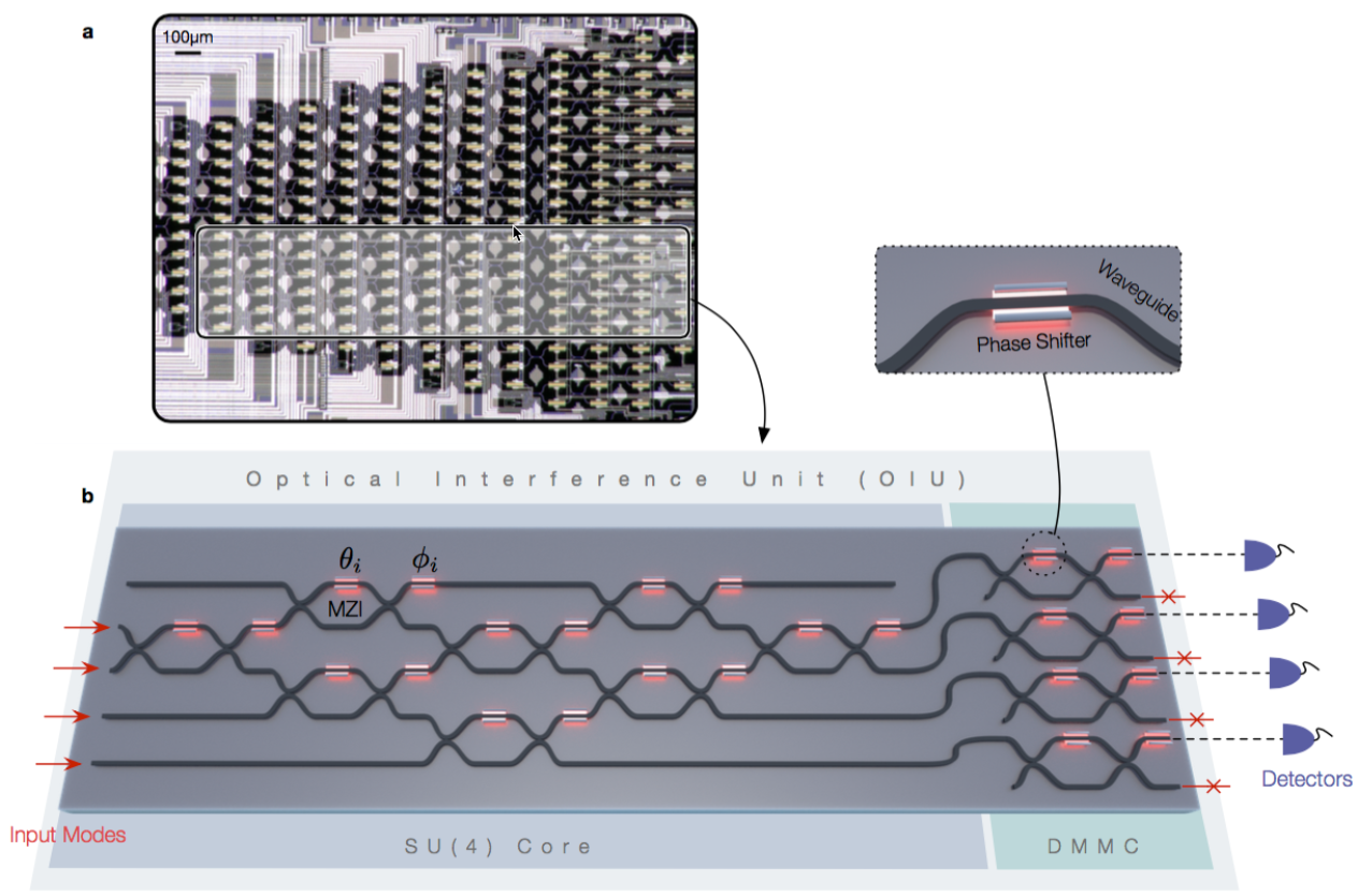
(a) Optical micrograph of an experimentally fabricated on-chip optical interference unit; the physical region where the optical neural network program exists is highlighted in gray. A programmable nanophotonic processor uses a field-programmable gate array (similar to an FPGA integrated circuit ) — an array of interconnected waveguides, allowing the light beams to be modified as needed for a specific deep-learning matrix computation. (b) Schematic illustration of the optical neural network program, which performs matrix multiplication and amplification fully optically. (credit: Yichen Shen et al./Nature Photonics)

A team of researchers at MIT and elsewhere has developed a new approach to deep learning systems — using light instead of electricity, which they say could vastly improve the speed and efficiency of certain deep-learning computations.

Deep-learning systems are based on artificial neural networks that mimic the way the brain learns from an accumulation of examples. They can enable technologies such as face- and voice-recognition software, or scour vast amounts of medical data to find patterns that could be useful diagnostically, for example.

But the computations these systems carry out are highly complex and demanding, even for supercomputers. Traditional computer architectures are not very efficient for calculations needed for neural-network tasks that involve repeated multiplications of matrices (arrays of numbers). These can be computationally intensive for conventional CPUs or even GPUs.

Programmable nanophotonic processor

Instead, the new approach uses an optical device that the researchers call a “programmable nanophotonic processor.” Multiple light beams are directed in such a way that their waves interact with each other, producing interference patterns that “compute” the intended operation.

The optical chips using this architecture could, in principle, carry out dense matrix multiplications (the most power-hungry and time-consuming part in AI algorithms) for learning tasks much faster, compared to conventional electronic chips. The researchers expect a computational speed enhancement of at least two orders of magnitude over the state-of-the-art and three orders of magnitude in power efficiency.

“This chip, once you tune it, can carry out matrix multiplication with, in principle, zero energy, almost instantly,” says Marin Soljacic, one of the MIT researchers on the team.

To demonstrate the concept, the team set the programmable nanophotonic processor to implement a neural network that recognizes four basic vowel sounds. Even with the prototype system, they were able to achieve a 77 percent accuracy level, compared to about 90 percent for conventional systems. There are “no substantial obstacles” to scaling up the system for greater accuracy, according to Soljacic.

The team says is will still take a lot more time and effort to make this system useful. However, once the system is scaled up and fully functioning, the low-power system should find many uses, especially for situations where power is limited, such as in self-driving cars, drones, and mobile consumer devices. Other uses include signal processing for data transmission and computer centers.

The research was published Monday (June 12, 2017) in a paper in the journal Nature Photonics (open-access version available on arXiv).

The team also included researchers at Elenion Technologies of New York and the Université de Sherbrooke in Quebec. The work was supported by the U.S. Army Research Office through the Institute for Soldier Nanotechnologies, the National Science Foundation, and the Air Force Office of Scientific Research.

Abstract of Deep learning with coherent nanophotonic circuits

Artificial neural networks are computational network models inspired by signal processing in the brain. These models have dramatically improved performance for many machine-learning tasks, including speech and image recognition. However, today’s computing hardware is inefficient at implementing neural networks, in large part because much of it was designed for von Neumann computing schemes. Significant effort has been made towards developing electronic architectures tuned to implement artificial neural networks that exhibit improved computational speed and accuracy. Here, we propose a new architecture for a fully optical neural network that, in principle, could offer an enhancement in computational speed and power efficiency over state-of-the-art electronics for conventional inference tasks. We experimentally demonstrate the essential part of the concept using a programmable nanophotonic processor featuring a cascaded array of 56 programmable Mach–Zehnder interferometers in a silicon photonic integrated circuit and show its utility for vowel recognition.

References from:
http://www.kurzweilai.net/learning-with-light-new-system-allows-optical-deep-learning

Yichen Shen et al. Deep learning with coherent nanophotonic circuits. Nature Photonics (2017) doi:10.1038/nphoton.2017.93

First In-Depth Look at Google’s New Second-Generation TPU

It was only just last month that we spoke with Google distinguished hardware engineer, Norman Jouppi, in depth about the tensor processing unit used internally at the search giant to accelerate deep learning inference, but that device—that first TPU—is already appearing rather out of fashion.

This morning at the Google’s I/O event, the company stole Nvidia’s recent Volta GPU thunder by releasing details about its second-generation tensor processing unit (TPU), which will manage both training and inference in a rather staggering 180 teraflops system board, complete with custom network to lash several together into “TPU pods” that can deliver Top 500-class supercomputing might at up to 11.5 petaflops of peak performance.

“We have a talented ASIC design tea that worked on the first generation TPU and many of the same people were involved in this. The second generation is more of a design of an entire system versus the first, which was a smaller thing because we were just running inference on a single chip. The training process is much more demanding, we need to think holistically about not just the underlying devices, but how they are connected into larger systems like the Pods,” Dean explains.

We will follow up with Google to understand this custom network architecture but below is what were able to glean from the first high-level pre-briefs offered on the newest TPU and how it racks and stacks to get that supercomputer-class performance. Google did not provide the specifications of the TPU2 chip or its motherboard, but here is the only image out there that we can start doing some backwards math with.


full post:  https://www.nextplatform.com/2017/05/17/first-depth-look-googles-new-second-generation-tpu/